DIGITAL ELECTRONICS & DESIGN ASPECTS
SEM-III, 2012-13
B.TECH EXAMINATION
UTTARAKHAND TECHNICAL UNIVERSITY
Time: 3 Hours
Total Marks: 100
Attempt any four parts of the following:
- Determine the base b in each of the following cases:
(a) (361)10 = (551)b
(b) (859)10 = (5B7)b - Write the 8-bit signed magnitude , 2's complement and 1's complement from the following decimal numbers:
(a) +119
(b) -77 - Write out the first ten number for a decimal weighted codes: 7, 4, 2, 1
- Using the theorems of Boolean algebra simplify the following expression:
- What is difference between a Latch and a flip-flop?
- What is race around condition and how it is overcome?
Attempt any two parts of the following:
- Construct a truth table for the following functions and from the truth table obtain an expression for the inversefunction:
- For the following two 4-variable functions
f2 = A + C +BD
how many of the input minterms are included in each of these functions and how many are not? What are the minterms expressions for the two functions? Simplify both functions using the theorems of Boolean algebra. - Simplify the following three-variable Boolean function algebraically and express them in terms of product of maxterms:
(a) f1 = ∑(1,2,5,6)
(b) f2 = ∑(0,1,2,3,7)
Attempt any two parts of the following:
- Minimize the following function and implement the minimized function using only NAND gates:
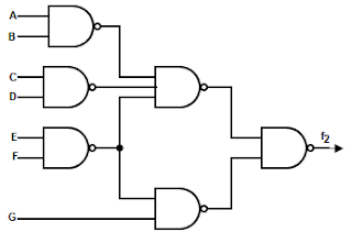
f(A, B, C ,D) = ∑(0, 2, 8, 9, 10, 12, 13, 14) - Analyze the circuit shown in fig. 1 to produce Boolean algebraic expression for the circuit outputs.
Fig. 1 - Implement the following function using only NOR gates having a maximum fan-in of three:
Attempt any two parts of the following:
- Implement the following 3-variable Boolean function using 4-input multiplexers:
f = ∑(0, 2, 3, 5, 7), control variable A and B. - Design a circuit for converting from the 8421 code to the 5421 code and implement the design with 4-to-1 multiplexers.
- Develop a 3-to-8 line decoder using NOR gates only, and draw its logic diagram.
Attempt any four parts of the following:
- Differentiate between the working of static and dynamic memory. Also discuss the difference between SRAM and DRAM.
- Design a synchronous modulo-12 counter using NAND gates and T flip-flops.
- Design a hazard-free, D-type flip-flop using asynchronous circuit design techniques. If may be assumed that the output will take on the value of the input on the trailing edge of a clock pulse.


